AAO Wafer has a unique, nanoscale material architecture exploited in a variety of industries and scientific fields toward the development of material science and nanotechnology. These are finding increased demand due to the high surface area and tunability of pore sizes of AAO, from electronics and energy storage to biomedicine. It is mainly due to growing research and development activities for better options because of competition, the growing consumer electronics industry globally, and a surge in support provided by financial institutions for advancements in nanotechnology, resulting in high demand for miniature devices.
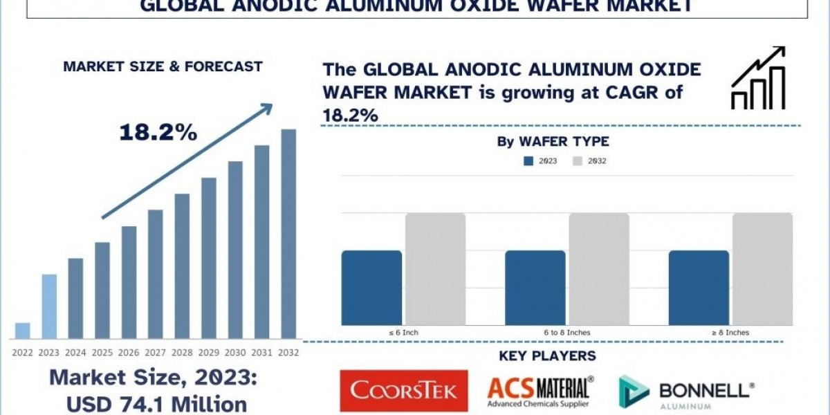
The growth in the renewable energy sector and the expansion of the biotechnology & medical devices industry would drive the global scenario of the Anodic Aluminum Oxide Wafer Market, according to analysis by Universal Data Solutions. According to their "Anodic Aluminum Oxide Wafer Market" report, the global market was valued at USD 74.1 Million in 2023, with an expected compounded annual growth rate of 18.2% during the forecast period from 2024 - 2032.
Request Free Sample Pages with Graphs and Figures Here - https://univdatos.com/get-a-free-sample-form-php/?product_id=65174
As a result, huge investments have been made in the market for improving production capacity and technology. Much prominence has been given to cost reduction and high-precision-manufacturing processes. Development in recent times has been related to the usage of AAO wafers in energy-efficient electronics and advanced sensor technologies. The expanding spectrum of application areas for AAO wafers has pushed businesses to explore their integration into new domains like healthcare and environmental monitoring, further extending the market's reach. AAO wafer market dominated by technologically advanced countries such as the US, China, and Japan, will further increase due to continuous R&D of advanced chipsets with high-quality transistors. Nanopore technology will play both a bad and a good role since it too will drive growth and sales. Still on the high would be renewable energy use, environmental technologies, and smart devices, with policies for the encouragement of innovation and sustainability such as investment by the US Department of Energy in nanotechnology for renewable clean energy solutions.
Growth in Renewable Energy Sector
This has been occasioned by the fact that the world is shifting towards the use of renewable sources of energy and therefore the need for materials that would improve efficiency of the energy conversion and storage systems. AAO wafers are also finding their applications in the renewable energy industry where there is high demand for surfaces with large surface area and controlled pore size for applications in solar cell and energy storage systems. In the case of solar cells, AAO wafers help as substrates for producing assorted nanostructures, which facilitate light trapping and enhance energy conversion efficacy hence boosting power conversion of photovoltaic systems. In the same way, the use of AAO as the anode or electrode for batteries and supercapacitors the porous structure wafers helps transfer ions more freely and store more energy density and enables a faster charging process.
For instance: Renewable energy sector wafers in AAO include their use in fabrication of dye-sensitized solar cells (DSSCs). Scholars have employed the AAO wafers as molds to fabricate P25-TiO2 nanostructured photoanodes that enhance the light absorption capacity of DSSCs. This innovation has the potential of enhancing economies of scale in solar energy technologies hence encouraging the adoption of renewable energy.
Increased Research and Development Activities
The growing interest in material science and nano fabrication is considered as a major reason for growth of R&D activities associated with Anodic Aluminium Oxide (AAO) wafers. Hence, with the flexibility of employing AAO as a template material and the capability of forming organizable nanostructures, AAO becomes the research focus. This has made it possible to discover new uses of AAO wafers as well as improving the features of existing technologies hence increasing the utilization of AAO wafers. The research and development efforts are focused on the application of AAO wafers in optoelectronics, electronics, and biotechnology; to produce newer generation devices with improved performance and characteristics.
For example, Research & Development is encouraging the proposed application of AAO wafers in fabrication of superior performance nanostructured sensors. The possibility of applying templates synthesized in AAO structures for creating nanosensors with high sensitivity and selectivity to the environment, medical diagnostics, and technical process control have stimulated the interest of the research institutions and companies. These innovations are not only paving way for new use of AAO wafers but are also integrating technology into the society in other fields.
Related Reports-
Anodic Aluminum Oxide Wafer Market: Current Analysis and Forecast (2024-2032)
Aluminium Nitride Market: Current Analysis and Forecast (2024-2032)
Expansion of the Biotechnology and Medical Devices Industry
The biotechnology and the medical devices industry has been growing at a very fast pace and there is need to come up with new materials to support the development of better healthcare products. The most widely used substrates in this industry include Anodic Aluminum Oxide (AAO) wafers, which have biocompatible properties, high chemical stability, as well as well-defined nanostructures that are desirable for biosensor, drug delivery and tissue engineering applications. The reporters in biosensors benefit from AAO wafers since they allow distinction of biological molecules such as proteins by their uniform pore structure, while the drug delivery systems benefit from AAO wafers since they allow for the controlled release of therapeutic agents. Another factor that is contributing to increase in demand for AAO wafers in the medical industry is called up personalized medicine and diagnostics.
For instance: Some of the uses of AAO wafers include in the industry of biotechnology as well as the medical devices industry, mainly in implantation of delivery systems of medicines. Such systems utilize the nature of porous AAO wafers to control the rate and duration of drug delivery to the disease site within the body, thus increasing therapeutic outcomes and at the same time minimizing side effects. As demonstrated in this application, AAO wafers may greatly transform the course of medical treatments and benefit the patients.
Conclusion
Overall, current trends point to the AAO Wafer's wide usage in a couple of high-impact industries like the renewable energy industry, increased research and development pursuits, and the biotechnology and medial devices industries. Their unique properties, including high surface area, controlled porosity, and biocompatibility, ensure progress in a variety of solar energy fields, nanostructured sensors, and novel treatments in health care. With AAO wafers playing a central role in technological development-from developing high-performance dye-sensitized solar cells and nanosensors to the fabrication of implantable drug delivery systems-continuously changing the face of such dynamic industries will only increase their importance and applicability, making AAO wafers a staple material in the progress and innovation of advanced technologies.